mobile background

Silicon Wafer CMP Slurry


Silicon Wafer CMP Slurry Series


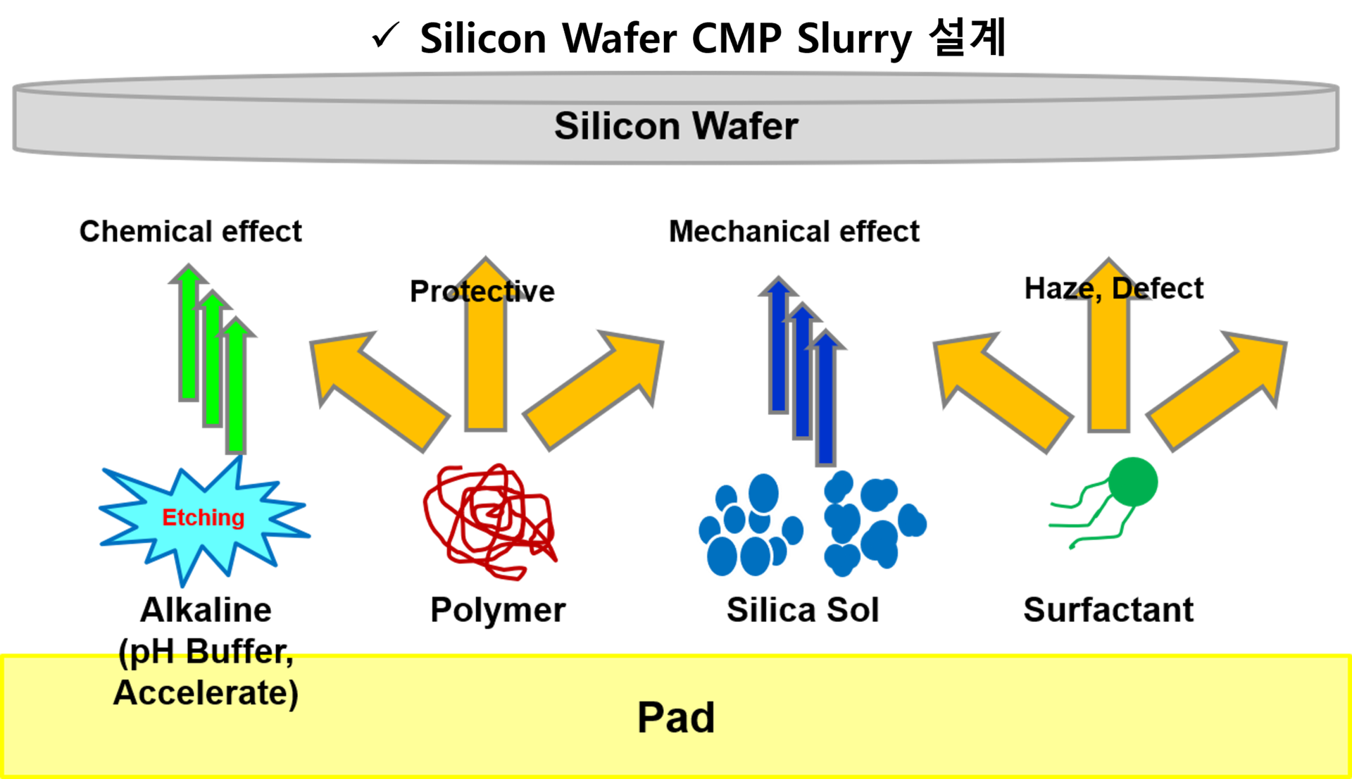
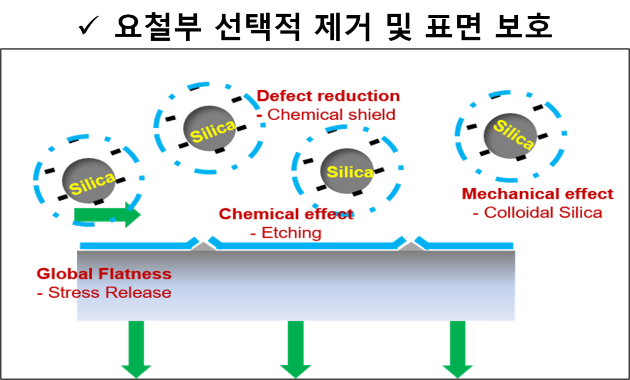
This is a chemical mechanical planarization (CMP) slurry used to achieve ultra-precise surface planarization in the silicon wafer manufacturing process. Its purpose and required characteristics differ somewhat from CMP slurries used in semiconductor device fabrication processes. 

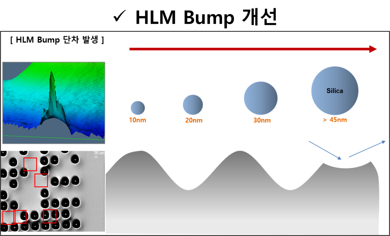
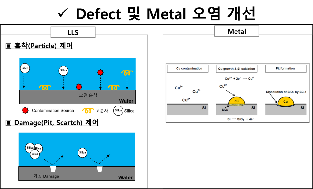
The primary roles of silicon wafer CMP slurry include silicon wafer surface planarization, removal of saw marks and lapping damage, control of surface roughness (Ra), improvement of Total Thickness Variation (TTV), minimization of warp and bow, and reduction of defects (scratches, pits, haze). Featuring these characteristics, silicon wafer CMP slurry is used in the final polishing step of the wafer manufacturing process, serving as a key material to produce high-quality mirror wafers for semiconductor device fabrication. 

In particular, colloidal silica-based slurries can achieve low defect rates and superior surface quality simultaneously, making them the most widely used choice in 200 mm and 300 mm silicon wafer manufacturing.   


View Details


[Product Inquiry]

Choi Dong-rak  PL   :  drchoi@acenanochem.com

Lee Jeong-pil  Pro :  jplee@acenanochem.com


Company Name  : ACE nanochem Co., Ltd. ㅣ CEO: Jonghoon Lee  ㅣ 

Business Registration Number  : 515-81-39501

Ace Nanochem Co., Ltd. Yeongcheon Plant (HQ) 

217 and 229, Yeongcheonsandan-ro, Geumho-eup, Yeongcheon-si, Gyeongsangbuk-do, Republic of Korea ㅣ Tel. +82-54-334-6240 ㅣ Fax. +82-54-334-6849 

Ace Nanochem Co., Ltd. Gyeongsan Plant (CMP R&D Center)

33, Jaingongdan-ro, Jain-myeon, Gyeongsan-si, Gyeongsangbuk-do, Republic of Korea ㅣ Tel. +82-53-857-6240 ㅣ Fax. +82-53-856-6849  

Chief Privacy Officer: Jueon Song  ㅣ Web Hosting Provider : LifeApp